The DMN32D4SDW-7 from Diodes Incorporated is an N-channel enhancement-mode MOSFET optimized for high-speed switching and low on-resistance in low- to medium-voltage applications. It is designed for efficient power management, load switching, and voltage regulation in compact, surface-mount applications. The device is fabricated using advanced planar technology to provide low gate charge, fast switching capability, and high current handling, making it suitable for DC-DC converters, synchronous rectification, load switches, and battery management systems. Its combination of low on-resistance, low gate threshold voltage, and thermal stability ensures minimal conduction and switching losses, allowing efficient operation in both industrial and consumer electronics designs.
## Device Overview
The DMN32D4SDW-7 is an N-channel MOSFET with a maximum drain-to-source voltage of 40 V and a continuous drain current rating of 32 A under specific thermal conditions. It features a very low on-resistance of 4.0 mΩ typical at VGS = 10 V, which minimizes conduction losses and heat generation during high-current operation. The device’s low gate charge and fast switching times allow high-efficiency operation at switching frequencies typical in modern DC-DC converters and synchronous rectifiers. It is provided in a compact SON (Small Outline No-lead) package, enabling high-density PCB layout and low parasitic inductance, essential for high-speed switching applications.
## Key Features
* MOSFET type: N-channel enhancement-mode
* Drain-to-source voltage (VDS): 40 V maximum
* Continuous drain current (ID): 32 A typical at 25°C, PCB dependent
* Pulsed drain current (IDM): 128 A maximum
* On-resistance (RDS(on)): 4.0 mΩ typical at VGS = 10 V, ID = 16 A
* Gate-to-source voltage (VGS): ±20 V maximum
* Total gate charge (Qg): 18 nC typical at VGS = 10 V
* Input capacitance (Ciss): 1200 pF typical
* Fast switching: rise time (tr) 12 ns typical, fall time (tf) 10 ns typical
* Low gate threshold voltage (VGS(th)): 1.2 V typical
* High thermal performance: junction-to-ambient RθJA = 40°C/W typical in SON package
* Compact SON-8 package for surface-mount applications
* Operating junction and storage temperature: -55°C to +150°C
## Electrical Characteristics
* Drain-to-source breakdown voltage (VDS): 40 V minimum at ID = 250 µA
* Gate threshold voltage (VGS(th)): 1.0–1.5 V at ID = 250 µA
* On-resistance (RDS(on)): 4.0 mΩ typical at VGS = 10 V, ID = 16 A
* Zero gate voltage drain current (IDSS): 1 µA maximum at VDS = 32 V, VGS = 0 V
* Forward transconductance (gfs): 55 S typical at VDS = 5 V, ID = 16 A
* Input capacitance (Ciss): 1200 pF typical
* Output capacitance (Coss): 450 pF typical
* Reverse transfer capacitance (Crss): 170 pF typical
* Total gate charge (Qg): 18 nC typical at VGS = 10 V, VDS = 32 V
## Switching Characteristics
* Rise time (tr): 12 ns typical at VDS = 32 V, ID = 16 A
* Fall time (tf): 10 ns typical under same conditions
* Turn-on delay time (td(on)): 7 ns typical
* Turn-off delay time (td(off)): 8 ns typical
* Fast switching capability enables operation at high frequencies up to several MHz
* Low gate charge and low input capacitance minimize switching losses in synchronous applications
## Thermal and Reliability Characteristics
* Maximum junction temperature (TJ): 150°C
* Storage temperature range (Tstg): -55°C to +150°C
* Thermal resistance junction-to-ambient (RθJA): 40°C/W typical in standard PCB layout
* Junction-to-case thermal resistance (RθJC): 1.2°C/W typical
* Efficient heat dissipation is enhanced by the SON package, which provides a low-thermal-resistance path for high-current operation
## Protection Features
* Robust VGS rating prevents gate oxide damage due to overvoltage
* Low RDS(on) minimizes thermal stress under heavy load conditions
* Capable of handling pulsed current up to 128 A without immediate failure
* High dv/dt tolerance reduces susceptibility to parasitic oscillations in fast-switching circuits
* Stable operation over full temperature and voltage range ensures reliable system performance
## Application Considerations
The DMN32D4SDW-7 is suitable for power management, load switching, and synchronous rectification in compact surface-mount designs. Proper layout techniques, including wide copper traces for the drain and source terminals and minimal parasitic inductance on the gate drive loop, are critical to achieving maximum efficiency and minimizing switching losses. Selection of gate drive voltage between 10 V and 12 V ensures full enhancement of the channel and minimal RDS(on). Attention to thermal management, including PCB copper area and potential heat sinking, is required when operating near maximum current ratings. It is ideal for battery-powered devices, point-of-load converters, DC-DC regulators, power distribution switches, and motor drive applications.
## Package Information
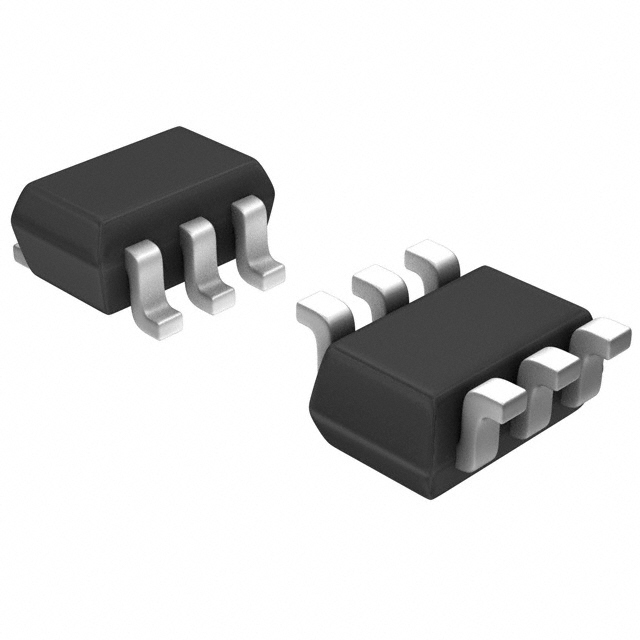
The device is housed in a compact SON-8 surface-mount package, providing low-profile mounting and efficient thermal dissipation. Its small footprint allows high-density board designs, while exposed pad design provides a low-thermal-resistance path to the PCB for heat removal. Pinout includes gate, source, and drain terminals optimized for minimal inductance and fast switching performance.
## Summary
The Diodes Inc DMN32D4SDW-7 is a high-performance N-channel MOSFET designed for low-voltage, high-current switching applications. With a 40 V VDS rating, very low RDS(on) of 4 mΩ, fast switching characteristics, and a compact SON-8 package, it is ideal for power management, synchronous rectification, and load switching in industrial and consumer electronics. Its low gate charge, high thermal performance, and robust design enable efficient, reliable operation in compact surface-mount circuits.