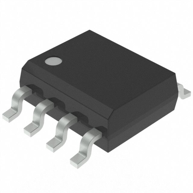
The ATTINY1617-MFR is an 8-bit microcontroller from Microchip Technology's AVR® ATtiny 1-Series family. It is built around the modern AVR CPU architecture and is intended for low-cost embedded control applications requiring a combination of compact size, low power consumption, integrated analog functionality, flexible digital peripherals, and efficient real-time operation. The device integrates Flash program memory, SRAM, EEPROM, configurable logic resources, timer peripherals, communication interfaces, and analog subsystems into a single-chip solution. The ATTINY1617-MFR is supplied in a compact package option suitable for space-constrained designs and is targeted toward industrial control, consumer electronics, sensor interfaces, smart appliances, lighting systems, and general-purpose embedded applications.
## Core Architecture and Processing Capability
The ATTINY1617-MFR is based on the AVR enhanced RISC architecture. The CPU executes most instructions in a single clock cycle, providing efficient processing performance for embedded control tasks. The architecture incorporates a register-based design that minimizes memory access overhead and improves execution efficiency.
The device operates at clock frequencies up to 20 MHz and supports deterministic interrupt handling through a vectored interrupt system. The combination of compact instruction encoding and efficient execution enables effective implementation of control algorithms, communication stacks, timing functions, and sensor-processing applications.
The microcontroller integrates 16 KB of in-system programmable Flash memory for application code storage. Volatile data storage is provided by 2 KB of SRAM, while 256 bytes of EEPROM support non-volatile storage of configuration parameters, calibration data, and user settings.
The memory architecture supports self-programming functionality, enabling firmware updates under software control when required by the application.
## Power Supply and Low-Power Characteristics
The ATTINY1617-MFR operates over a supply voltage range of 1.8 V to 5.5 V. This wide operating range allows direct integration into both battery-powered systems and conventional regulated embedded platforms.
A significant characteristic of the ATtiny 1-Series family is its low-power design. Multiple sleep modes are available to reduce current consumption during inactive periods while preserving critical functionality. Peripheral modules can remain operational during specific low-power states, allowing event-driven operation without continuous CPU activity.
Integrated brown-out detection circuitry supports reliable operation during supply-voltage transitions. Power-on reset functionality ensures controlled startup behavior following power application.
## Memory and Non-Volatile Storage Resources
The Flash memory subsystem provides storage for application firmware and supports in-system programming through standard programming interfaces.
The EEPROM subsystem allows data retention independent of program memory. This capability is particularly useful for storing user preferences, operating parameters, calibration coefficients, and system configuration values that must survive power cycling.
The SRAM memory provides temporary storage for variables, communication buffers, stack operations, and runtime data processing. The memory organization is optimized for efficient access by the AVR CPU architecture.
## Analog Peripheral Integration
The ATTINY1617-MFR includes a comprehensive analog subsystem that enhances its suitability for mixed-signal embedded applications.
A 10-bit Analog-to-Digital Converter supports multiple analog input channels and can be used for measurement of sensor outputs, supply voltages, environmental parameters, and user-interface signals. The ADC architecture supports flexible reference-voltage selection and event-driven operation.
An analog comparator is integrated for threshold detection, voltage monitoring, protection circuits, and timing-sensitive control functions. The comparator can operate independently of the CPU, enabling rapid hardware-based response to analog events.
The device also incorporates an internal temperature sensor that can be used for system monitoring and temperature-dependent control functions.
## Timer and Control Peripherals
The timer subsystem includes both Timer/Counter Type A (TCA) and Timer/Counter Type B (TCB) peripherals. These resources support interval timing, event counting, waveform generation, frequency measurement, pulse-width modulation generation, and capture/compare functions.
The TCA peripheral is capable of generating multiple PWM outputs for motor control, LED dimming, power regulation, and actuator control applications.
The TCB peripherals provide flexible timing resources suitable for pulse measurement, signal generation, and protocol timing functions.
A Real-Time Counter (RTC) is also integrated, enabling low-power timekeeping and periodic wake-up functionality.
## Event System and Configurable Logic
One of the distinguishing characteristics of the ATtiny 1-Series architecture is its Event System. This hardware mechanism allows peripheral modules to communicate directly without CPU intervention.
Events generated by timers, communication interfaces, analog peripherals, or external inputs can trigger actions in other peripherals with minimal latency and reduced power consumption. This capability enables highly efficient real-time control implementations.
The device additionally incorporates Configurable Custom Logic (CCL) blocks. These hardware logic resources allow implementation of simple combinational and sequential logic functions directly within the microcontroller, reducing software overhead and minimizing external component requirements.
## Communication Interfaces
The ATTINY1617-MFR provides multiple communication interfaces for integration into embedded systems.
The Universal Synchronous and Asynchronous Receiver Transmitter (USART) supports serial communication with external devices such as sensors, displays, wireless modules, and host processors.
A Serial Peripheral Interface (SPI) module enables high-speed communication with memories, converters, displays, and peripheral controllers.
An Inter-Integrated Circuit (I²C) compatible Two-Wire Interface (TWI) supports communication with a broad range of digital sensors, EEPROM devices, real-time clocks, and control circuits.
These communication resources allow the microcontroller to serve as a central control element within distributed embedded architectures.
## Input and Output Characteristics
The ATTINY1617-MFR provides multiple general-purpose input/output pins with flexible configuration capabilities.
Each pin can be configured for digital input, digital output, peripheral function operation, or analog input use depending on system requirements. Internal pull-up resistors are available to simplify external circuitry.
External interrupt capability allows rapid response to asynchronous events. Pin multiplexing enables efficient utilization of package resources by allowing several peripheral functions to share common physical pins.
The I/O architecture is designed to support direct interfacing with sensors, switches, LEDs, communication devices, and external control circuits.
## Safety, Reliability, and Development Features
The microcontroller incorporates a Watchdog Timer that can automatically recover the system from software execution faults. Windowed watchdog functionality provides additional monitoring capability for safety-critical applications.
Clock monitoring mechanisms help ensure reliable operation under abnormal clock conditions. Multiple internal oscillator options reduce dependence on external timing components while simplifying PCB design.
Programming and debugging are supported through the Unified Program and Debug Interface (UPDI), which provides a simplified single-wire programming and debugging solution.
## Package Characteristics and Application Areas
The ATTINY1617-MFR is supplied in a compact package suitable for high-density PCB layouts and space-constrained products. The package provides access to the device's digital, analog, communication, and control resources while maintaining efficient board utilization.
Typical applications include sensor nodes, smart lighting systems, appliance controls, battery-powered devices, industrial monitoring equipment, motor-control subsystems, user-interface controllers, portable instrumentation, IoT edge devices, environmental monitoring systems, and general-purpose embedded control products.
The combination of a 20 MHz AVR CPU, 16 KB Flash memory, 2 KB SRAM, EEPROM storage, integrated ADC, configurable logic, event-driven architecture, multiple communication interfaces, and low-power operating modes makes the ATTINY1617-MFR a highly integrated microcontroller solution for compact and cost-sensitive embedded designs.