Product Overview
The Texas Instruments TL494CDR is a highly versatile and widely used pulse-width modulation (PWM) control circuit, designed primarily for switching power supply and DC-DC converter applications. It integrates all the essential components for PWM control including error amplifiers, a dead-time control comparator, an oscillator, a 5 V reference regulator, and output transistors. This controller enables flexible design and precise control of the switching process, suitable for both voltage and current mode regulation schemes. It is fabricated using bipolar analog technology, ensuring high stability and low drift.
Key Features
* Internal 5 V Precision Reference Regulator
* Two Error Amplifiers for Feedback Control
* Adjustable Dead-Time Control
* Oscillator with Programmable Frequency
* Dual Output Transistors with Push-Pull or Single-Ended Configuration
* Wide Operating Temperature Range
* Short-Circuit and Overload Protection Capability via External Sensing
* Low Power Consumption
Applications
* Switch-mode power supplies (SMPS)
* DC-DC converters
* Battery chargers
* Motor control systems
* Inverters and UPS systems
* LED drivers
* Consumer electronics and industrial power control
Electrical Characteristics
| Parameter | Typical Value |
| ------------------------------------- | ----------------------------------------- |
| Supply Voltage Range (VCC) | 7 V to 40 V |
| Reference Output Voltage | 5 V ± 0.5% |
| Oscillator Frequency Range | 1 kHz to 300 kHz |
| Dead-Time Control Voltage Range | 0 V to 3.3 V |
| Output Collector Voltage | 40 V (max) |
| Output Emitter Current | 200 mA (max) per output |
| Output Saturation Voltage | < 1.3 V @ 200 mA |
| Input Offset Voltage | ±10 mV (typical) |
| Power Consumption (quiescent) | ~12 mW (typical) |
| Operating Temperature Range | 0°C to +70°C (commercial grade, TL494CDR) |
Functional Block Diagram Components
1. Voltage Reference
An internal 5 V reference regulator provides a stable supply for internal circuitry and external use. It is accurate within ±0.5% and can source up to 10 mA.
2. Error Amplifiers
Two differential error amplifiers with high gain allow implementation of closed-loop control schemes. Designers can use these to regulate output voltage or current depending on feedback network configuration.
3. Dead-Time Control Comparator
This comparator ensures that the two outputs do not conduct simultaneously, preventing cross-conduction in push-pull configurations. The dead-time is adjustable using a single external resistor or voltage applied to the DTC pin.
4. Oscillator
The internal oscillator frequency is set by an external resistor and capacitor connected to the RT and CT pins. It determines the PWM switching frequency and can be configured to operate from 1 kHz up to 300 kHz depending on the component values.
5. PWM Comparator and Latch
The PWM comparator compares the output of the error amplifier with a sawtooth waveform from the oscillator to determine pulse width. The latch ensures proper timing and synchronization of switching transitions.
6. Output Stage
The TL494 provides two totem-pole outputs which can be configured in either push-pull or single-ended mode. This flexibility allows use in various converter topologies such as forward, flyback, or half-bridge configurations.
7. Shutdown and Soft Start
The shutdown function is achieved by pulling the COMP pin low or applying a voltage to the DTC pin. This can be used for overvoltage, overcurrent, or thermal protection. Soft start can be implemented by controlling the COMP pin voltage during startup.
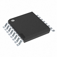
Pin Configuration (SOIC-16 - D Package)
| Pin | Name | Function |
| ------- | ----------- | ----------------------------------------------- |
| 1 | 1IN+ | Non-inverting input of Error Amp 1 |
| 2 | 1IN− | Inverting input of Error Amp 1 |
| 3 | FB | Output of Error Amp 1 / Input to PWM comparator |
| 4 | DTC | Dead-time control |
| 5 | CT | Timing capacitor for oscillator |
| 6 | RT | Timing resistor for oscillator |
| 7 | GND | Ground |
| 8 | C1 | Output control logic |
| 9 | E1 | Emitter of output transistor 1 |
| 10 | C2 | Collector of output transistor 2 |
| 11 | E2 | Emitter of output transistor 2 |
| 12 | VCC | Supply voltage |
| 13 | Output Ctrl | Push-pull or single-ended mode selection |
| 14 | REF | 5 V precision reference output |
| 15 | 2IN− | Inverting input of Error Amp 2 |
| 16 | 2IN+ | Non-inverting input of Error Amp 2 |
Design Considerations
* Frequency Selection: Choosing RT and CT values determines the oscillator frequency. For a switching frequency of 100 kHz, typical values might be RT = 10 kΩ and CT = 1 nF.
* Dead-Time Tuning: Adjusting the DTC pin voltage provides fine control of minimum output pulse width and protects against shoot-through in output switches.
* Thermal Management: Though the TL494 is efficient, systems operating in high ambient temperatures or at high switching frequencies may require PCB-level thermal considerations due to power dissipation in the output drivers.
* Output Drive Configuration: In push-pull mode, C1 and C2 alternate in driving the outputs; in single-ended mode, the outputs can be paralleled or used independently to drive external MOSFETs or BJTs.
Summary
The Texas Instruments TL494CDR is a time-proven PWM controller IC that combines versatility, stability, and ease of implementation. With a built-in reference, dual error amplifiers, adjustable oscillator, and dual output drivers, it supports a wide range of DC-DC and AC-DC conversion topologies. Its robustness, cost-effectiveness, and extensive use in commercial and industrial products have made it a foundational component in power electronics.