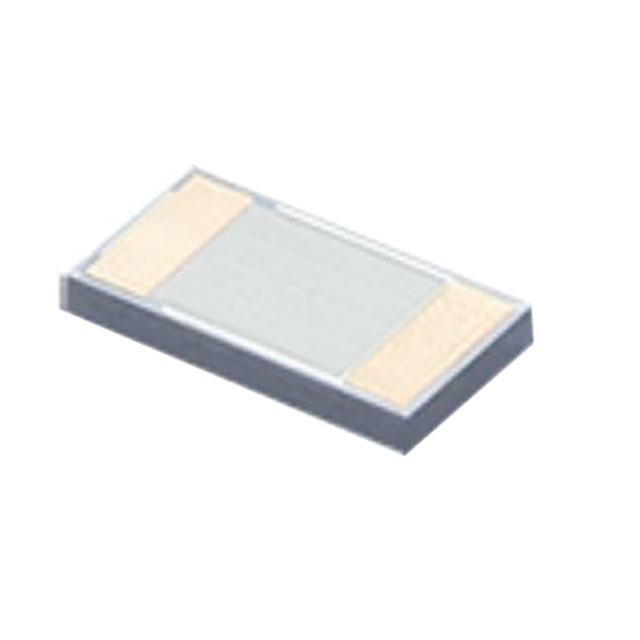
The Murata Manufacturing 935151424610-T3N is a surface-mount passive component developed for high-frequency and compact electronic systems requiring stable impedance characteristics, controlled parasitic behavior, and compatibility with automated PCB assembly processes. Based on Murata’s multilayer ceramic component manufacturing technologies, the device is intended for use in RF signal conditioning, filtering, impedance matching, suppression of conducted noise, and high-density electronic circuit integration. The component is engineered to maintain electrical stability across a specified operational frequency range while minimizing package-induced parasitic effects that could degrade signal integrity in modern high-speed or RF-oriented designs.
## Device Classification and Functional Positioning
The 935151424610-T3N belongs to the category of multilayer ceramic passive devices optimized for surface-mount implementation. Murata’s construction methodology for this class of components typically involves laminated ceramic dielectric layers combined with precision internal electrode structures to achieve compact dimensions and repeatable electrical characteristics. The device is intended for applications where low-profile mounting, high packing density, and stable frequency-domain behavior are required.
From a circuit-function perspective, the component operates as a passive impedance element whose electrical response is frequency-dependent. Depending on the surrounding topology, it may serve functions such as attenuation of unwanted high-frequency energy, shaping of transfer functions, RF decoupling, resonance network formation, or suppression of electromagnetic interference. The passive structure contains no active switching or amplification mechanisms, ensuring predictable linear behavior within its rated operating conditions.
The tape-and-reel suffix designation indicates packaging optimized for automated pick-and-place assembly equipment. This is important in high-volume electronics manufacturing environments where placement accuracy, solderability consistency, and thermal process compatibility directly influence production yield and long-term field reliability.
## Electrical Characteristics
The electrical behavior of the 935151424610-T3N is defined by its nominal impedance-related parameter, tolerance range, equivalent series resistance characteristics, and frequency response profile. In multilayer ceramic passive devices, these parameters are tightly coupled to the internal electrode geometry, dielectric formulation, and conductor material composition.
The component exhibits controlled parasitic inductance and capacitance characteristics appropriate for high-frequency circuit implementation. At lower frequencies, the device behavior follows its intended passive model with predictable impedance characteristics. As operating frequency increases, distributed parasitic elements become increasingly significant, requiring designers to evaluate insertion loss, resonant behavior, and impedance variation across the intended operational spectrum.
DC resistance characteristics are minimized through optimized internal conductor structures, reducing conductive loss and thermal dissipation during operation. This contributes to improved efficiency in filtering and RF energy transfer applications. Frequency-dependent impedance stability is particularly important in communication equipment, clock-distribution circuits, and switching regulator noise suppression networks where uncontrolled impedance drift can compromise system performance.
The self-resonant behavior of the component establishes the upper frequency region where the intended passive characteristic transitions due to interaction between internal inductive and capacitive parasitics. Proper circuit implementation therefore requires operation within the effective region defined by the component’s intended electrical model.
## Thermal and Environmental Operating Conditions
The device is designed for operation across an industrially relevant temperature range compatible with standard electronic assemblies. Electrical characteristics remain within specified limits when operated inside the rated environmental envelope. Thermal stability is achieved through ceramic material optimization and internal electrode configuration, reducing drift caused by temperature-dependent dielectric variation.
The component is intended for compatibility with standard lead-free reflow soldering profiles used in SMT manufacturing. Excessive thermal gradients during soldering or improper board handling can induce mechanical stress in multilayer ceramic structures, making PCB layout and assembly profile control important reliability considerations.
Humidity exposure, thermal cycling, and mechanical vibration tolerance are addressed through the intrinsic robustness of the ceramic multilayer construction. However, long-term reliability depends on maintaining operating conditions within specified voltage, current, and environmental limits. Excessive board flexure during depanelization or connector insertion can mechanically stress ceramic passive components, potentially affecting structural integrity or electrical performance.
## Signal Behavior and Interfacing Characteristics
As a passive two-terminal device, the 935151424610-T3N does not incorporate logic-state interpretation or active signal processing functionality. Its interaction with external circuitry is governed entirely by impedance characteristics and frequency-domain response.
When integrated into RF or high-speed digital systems, the device contributes to signal conditioning by modifying spectral content, attenuating unwanted noise, or stabilizing impedance discontinuities. In filtering applications, the component operates in conjunction with capacitive or inductive network elements to establish defined cutoff frequencies or resonant characteristics.
The absence of polarity sensitivity simplifies PCB orientation and assembly handling. Current flow through the device is bidirectional under AC conditions, and electrical behavior remains symmetric with respect to terminal orientation. This characteristic is advantageous in automated manufacturing environments and high-density PCB layouts.
At elevated frequencies, interconnect geometry, pad dimensions, and PCB ground referencing become significant contributors to overall circuit performance. Consequently, optimal implementation requires controlled PCB layout practices to minimize unintended parasitic coupling and preserve intended impedance characteristics.
## Typical Application Scenarios
The 935151424610-T3N is suitable for RF front-end circuitry where compact passive elements are required for impedance matching, harmonic attenuation, and signal-path conditioning. Wireless communication modules, antenna matching networks, and RF transceiver subsystems benefit from the stable high-frequency characteristics associated with multilayer ceramic passive technologies.
In power integrity applications, the component can be deployed within filtering networks intended to suppress conducted switching noise generated by DC-DC converters or high-speed digital logic. Its compact dimensions and SMT compatibility make it suitable for multilayer PCB architectures with stringent space constraints.
The device is also applicable in electromagnetic interference mitigation structures, particularly where high-frequency noise suppression must be achieved without introducing substantial conductive loss or occupying excessive board area. Consumer electronics, industrial controllers, communication infrastructure, and embedded processing systems commonly employ such passive components to maintain signal integrity and regulatory electromagnetic compatibility compliance.
## Mechanical Construction and Assembly Considerations
The multilayer ceramic construction provides a high volumetric efficiency relative to discrete wire-wound or larger passive alternatives. The external terminations are engineered for reliable solder wetting and mechanical attachment under standard SMT assembly conditions. Tape-and-reel packaging facilitates automated placement while minimizing handling-induced contamination or mechanical damage.
PCB land-pattern optimization is important to control solder joint stress distribution and maintain long-term mechanical reliability. Uneven solder fillets or excessive mechanical strain can produce localized stress concentrations within ceramic passive structures. Controlled reflow profiles and balanced PCB support reduce the likelihood of crack formation during manufacturing.
The low-profile geometry assists in minimizing loop inductance and improving high-frequency behavior, particularly in RF and decoupling applications where current return-path optimization is critical.
## Summary and Conclusion
The Murata Manufacturing 935151424610-T3N is a multilayer ceramic surface-mount passive component engineered for compact high-frequency electronic systems requiring stable impedance behavior, low parasitic effects, and reliable SMT assembly compatibility. Its electrical characteristics support filtering, impedance matching, RF conditioning, and EMI suppression functions across a broad range of embedded and communication-oriented applications.
The device combines controlled frequency-domain performance, minimized conductive losses, robust ceramic multilayer construction, and automated manufacturing compatibility. Proper implementation requires consideration of PCB layout, thermal assembly conditions, and high-frequency parasitic behavior to fully realize intended circuit performance. Within its specified operating limits, the 935151424610-T3N provides a reliable and space-efficient passive solution for modern high-density electronic designs.